Hacker's Guide to Making Circuit Boards (Part 1)
Hey! The purpose of this series is to teach you how to design, manufacture, and program a circuit board. Afterwards, you’ll be well positioned to work on a simple circuit board that drives something like bluetooth headphones, a quadcopter, or an electric skateboard.

The focus throughout the series is on teaching a small set of skills that can get you surprisingly far: the equivalent of pip install and for-loops for electrical engineering.
I’m still quite new to this, but making a circuit board is way easier than I thought before I started. I’ve written this tutorial with the goal of making it widely accessible. Notably,
- You don’t need to understand advanced stuff about circuits, like inductance. It might be useful if you remember some high school physics, like Ohm’s law, but you can pick this up as you need it. The most advanced individual circuits we’ll see look a lot like this.
- You don’t need to know how to solder. I don’t. You can get your boards manufactured overseas with all the components perfectly inserted and soldered by a machine.
- It doesn’t cost a lot of money. I spent less than $100 total on this project. That bought me five fully assembled boards and all the equipment necessary to program them. If you grew up with Arduino and SparkFun, you might be surprised (like I was) that a MPU6050 inertial measurement unit ($25 on a breakout board from SparkFun) actually costs $2 as a bare component (and less in bulk).
Concretely, we’ll be designing a circuit board that controls a robot. It’ll read data from a gyroscope and drive four servo motors. We’ll control it with a few buttons, power it with four AA batteries, and program it in Rust.
Let’s dive in!
Creating a Schematic
Our first order of business will be creating a schematic of our circuit board. A schematic is an abstract diagram that indicates which components we want to use, and how they should be electrically connected to one another.
Inertial Measurement Unit
The first component we’ll add to our schematic will be an inertial measurement unit (IMU). IMUs contain several sensors like gyroscopes and accelerometers integrated into a single chip, and tell you how fast you’re turning, where you’re pointing, and whether you’re accelerating.
We’ll start by choosing a specific IMU. Luckily, there’s a great third party comparison of the gyroscopes on many popular IMUs. You can go through this list and choose any that strikes your preferred price-performance-functionality tradeoff; we’ll go with the MPU 6050, which is a classic. [1]
Open up your schematic editor of choice (this tutorial uses EasyEDA [2]). Create a new schematic, then go to Place > Symbol, and search for the MPU 6050.
 Once you place it, you’ll see an abstract representation of the MPU 6050 with all its pins.
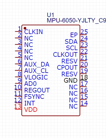 To figure out what these pins do, you’ll need to take a look at the part’s datasheet (Google is your friend). These tend to be long and verbose; the MPU6050 datasheet is more than 50 pages long. A good place to start is by looking at the pin out table.
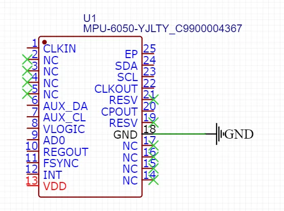
 This table describes the purpose of each of the pins on the bottom of the MPU6050. Some of these descriptions are self-explanatory; pin 18 is labelled “GND” and is supposed to be connected to ground. We can start by connecting that one in our schematic editor.
We can also put the X symbol on all eight NC pins and both RESV pins, which the pinout chart labels as “Not internally connected.” and “Reserved. Do not connect.” respectively. Although the X symbol doesn’t do anything, it’s a good reminder that we don’t need to connect anything there.
That’s where the Typical Operating Circuit comes in handy. This is a different diagram in the datasheet where the manufacturer basically lets you know how reasonable people set up their ICs. There might be three pages of information on which capacitor values are acceptable, but the typical operating circuit should give you reasonable defaults.
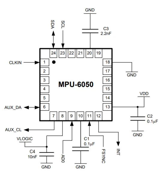 Here, we can see that pin 10 (REGOUT) is supposed to be connected to a 0.1uF capacitor and then to GND. Let’s add that to the schematic (recall that 0.1uF = 100nF).
You’ll notice that there are lots of 100nF capacitors in the parts library. The ones that we want are in the “Basic Part” class (these are much cheaper than the “Extended Part” versions in low volumes). The four basic 100nF capacitors differ in the 4-number code that comes afterward; those are sizes. We chose the 0603 size, which is 0.06 inches by 0.03 inches. Then we connect it to REGOUT on one side and ground on the other.
You might wonder what the purpose of this capacitor is. It’s called a bypass capacitor, which you can think of like a little backup battery kept close to the chip. When the electrical inputs to the chip are noisy, the bypass capacitors effectively absorb and supply power to smooth over those irregularities.
You can copy capacitors from the typical application circuit for VLOGIC, CPOUT, and VDD. What about the rest of the pins?
CLKIN and FSYNC say “optional, connect to ground if unused.” We’re not trying to do anything fancy, so we ground them.
SDA and SCL implement a communication protocol called I2C. We’ll use these two pins to send questions and instructions from our microcontroller to our MPU6050.
How do we send bits over these wires? We start by connecting SDA and SCL to +3.3v on the schematic. To send a logical zero, the microcontroller connects its side of the wire to ground internally, which forces the line to zero volts. To send a logical one, the microcontroller does nothing with the pin, and the +3.3v connection tugs the line high automatically.
There’s one catch. If you just connect +3.3v directly to ground inside your microcontroller, you have a short circuit and your chip will get hot and fry itself. To avoid this problem, we put a “pull-up” resistor between the power supply and the microcontroller. This sharply limits how much power an internal ground can pull from the 3.3v supply.
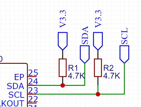
This all sounds complicated, but it’s not so bad once you do it once. Here’s how it’ll look when you’re done. Notice the 4.7K pull-up resistors between the power supply (V3.3) and the pins. The SDA and SCL labels will eventually connect to SDA and SCL pins on the microcontroller. The V3.3 label indicates a connection to +3.3 volts, supplied from somewhere else on the board.
 AUX_DA and AUX_CL are another I2C pair for “connecting external sensors,” which we don’t have. We shouldn’t leave them unconnected, since I2C lines need to be kept at 3.3v by default, so we connect them to our 3.3v power through another pair of 4.7k pull-up resistors.
AD0 controls the “I2C slave address LSB.” If you search the datasheet for AD0, you’ll find this diagram, which says that the MPU6050’s I2C address is 1101000 when AD0 is low, and 1101001 when AD0 is high. Either is fine for us; we’ll choose to set it low by connecting it to ground.
 INT is an interrupt pin; the gyroscope can activate it to quickly signal something like “this chip is in free-fall.” We won’t use it.
EP is on the schematic, but not on the datasheet pinout. Stack Exchange says that it refers to the big pad on the bottom of the chip, which should sometimes be soldered to ground as a heatsink. However, looking through the datasheet, we see:
 We therefore choose not to connect EP.
When all of that is said and done, your schematic should look something like this.
 Congratulations! You’ve set up your first chip.
Power (3.3v LDO)
We said before that the 3.3V label indicates a connection to +3.3 volts, generated somewhere else on the board. Let’s tackle that now.
The MPU6050 needs 3.3 volts to run, but we’re planning to run our controller on a set of four AA batteries, which together will output 4 * 1.5 volts = 6 volts.
To decrease the voltage from 6v to 3.3v, we’ll use a LDO (Low Dropout regulator). LDOs are simple, cheap, and inefficient: they take an unknown input voltage and output a constant output voltage. If we input 6 volts, our LDO should output 3.3 volts and burn off the other 2.7 volts as heat.
We’ll try to choose a popular and well-documented LDO, so go to this website and search for “3.3v LDO,” then sort down by stock. You’ll see at the top there are a bunch of 1117-series parts (notice how they all have 1117 in their part number).
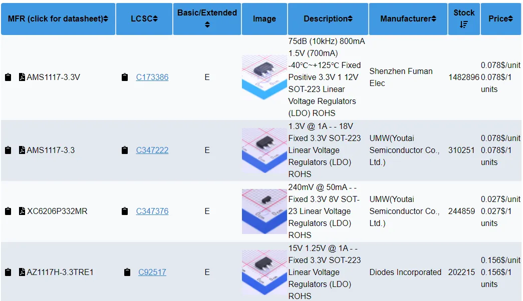 We’ll grab one of these 1117 chips. Digging through its datasheet, we find this wonderful typical operating circuit in Chinese.
 We copy that diagram into our schematic as follows.
Here’s our final LDO setup.

Battery Connector
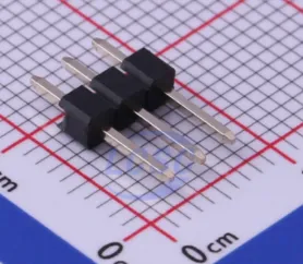
Next, we’ll connect the input side of the LDO to our battery with a battery connector. Our generic battery pack comes with a 2.54-mm spaced connector. Using the same parts website, I eventually found a matching header.
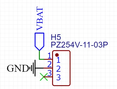
 It’s pretty simple to connect in the schematic. Make sure you put the VBAT connection on the + side of your battery, and the GND connection for the - side.
Microcontroller: Selection
Next we’ll select a microcontroller, which is the star of the show.
We’ll use a chip from the STM32 series, which is perhaps the most popular modern line of microcontrollers. More specifically, we’ll choose the STM32F3 series, which is based on a Cortex-M4 core (mid-range) and has floating point support. It also has a good Rust HAL for later!
Reading the STM32F3xx documentation page, it seems like the F302 is a standard choice without bells and whistles like high resolution timers.
Finally, the STM32F302 can be configured with varying amount of flash memory, RAM, and pins. We’ll ultimately go with the STM32F302C8T6, which has 64k of flash, 16k of RAM, and comes in a 48 pin package. Here she is:
 Phew! That’s a lot of pins to connect.
Microcontroller: Power
Let’s start with power. Looking at the STM32F3xx datasheet section on power supply, we see the following diagram. Fortunately, everything on the right is inside the microcontroller; we only have to worry about the left side.
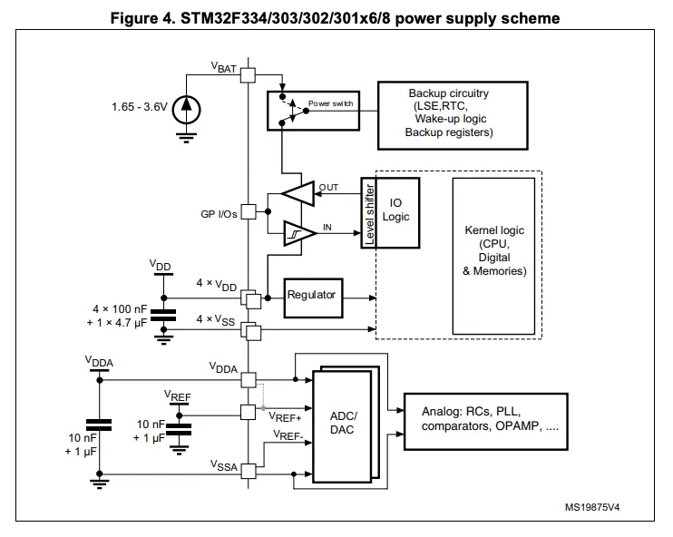 According to the top of the diagram, VBAT should be connected directly to the battery.
According to the middle of the diagram, we should connect each of the VDD pins to 3.3v, and each of the VSS pins to ground. We’re also supposed to add four 100nF and one 4.7uF bypass capacitors.
According to the bottom of the diagram, we should also attach VDDA and VSSA to power and ground respectively, with one 10nF and one 1uF capacitor. (If we wanted particularly accurate analog readings, we could take further care to isolate these pins from other electrical noise on the board.)
 The schematic can be deceiving; although these look like four separate circuits, the V3.3s and GNDs all link together. This is why it doesn’t matter that the 4.7uF capacitor is only graphically attached to the bottom pins; it’s electrically connected to all of them. [3]
Microcontroller: Clocks
The STM32F302 has high speed and low speed internal clocks. They’re not particularly accurate. If we need higher timing accuracy, we can choose to add external crystal oscillators to the OSC_IN, OSC_OUT, OSC32_IN, and OSC32_OUT pins. Since we don’t need particularly high timing accuracy, we’ll save the cost and leave these as generic I/O pins.
Microcontroller: Reset
We need a way to restart the microcontroller; that’s handled by the NRST pin.
 According to the STM32F302 datasheet, NRST is active low. This means that the pin should usually be high (at 3.3v). When we push the reset button, it should temporarily drop to ground to restart the board. We’ll do that with the following circuit.
 SW1 is a generic pushbutton; when you push, it connects the 1/2 side to the 3/4 side. By default, NRST is held to 3.3v, since it’s connected to V3.3 through that 47k resistor. When SW1 is held, NRST is also connected to ground through a 10k resistor. Since the ground resistor is smaller, the voltage on NRST jumps closer to ground. This gadget is called a voltage divider. [4]
Microcontroller: Boot
When the microcontroller starts, where should it execute code from? Most often, it should execute from main memory (where our programs are written). But sometimes we might want to boot from a stable system bootloader instead.
This choice is controlled by the Boot0 pin.
 So usually Boot0 should usually be low, corresponding to main flash memory, but when we hold a button, we’ll set Boot0 high to boot from system memory instead. We won’t worry about the third chart entry, embedded SRAM, for now.
To achieve this, we’ll use the same gadget we used for NRST, but with V3.3 and GND reversed.
 If we want to boot from system memory, we’ll hold down the SW2 button during boot up.
Microcontroller: Debug
Now we need a way to program our microcontroller. We’ll do that using a debug tool that speaks the SWD (serial wire debug) protocol. The connector for that tool is a 2x5 male header with 1.27mm spacing, laid out like this:
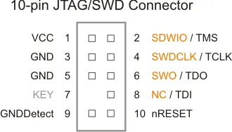 None of our microcontroller pins are labelled “SWDIO”, but we can reference this handy table to see which pin handles that function. In our case, it looks like the PA13 pin handles SWDIO.
 We also need to attach SWDCLK, SWO, and NRST. First we’ll put little tags on the relevant pins:
 Then we’ll grab a 2x5 pin header with 1.27mm spacing and attach those tags to it, along with power and ground.
 We now have the basics of the microcontroller fully configured. All that’s left is to attach inputs and outputs for the IMU and servos.
Microcontroller: IMU I2C
Recall that our IMU speaks to our microcontroller through the I2C protocol, using an SDA and an SCL pin. Where can we find SDA and SCL on our microcontroller?
Scrolling through the pinout table, we notice that PA10 has an alternate function as “I2C2_SDA”, and PA9 is similarly listed for “I2C2_SCL”. Since we don’t need PA9 and PA10 for anything else, we’ll use the second I2C interface, “I2C2”. (If we had needed PA9 for a different alternate function, we could have used I2C1 or I2C3 instead.)
 We connect PA9 and PA10 to the IMU with the same SDA and SCL tags we used back then.

Servos
Finally, for the servos. We can control servos by sending them pulses of varying lengths, using a system called pulse width modulation (PWM). We’ll discuss this more in part 3, when we program the microcontroller. For now, we need to take care to attach the servos to IO pins with the hardware needed to generate PWM signals.
Searching for “PWM” in the datasheet, we find the following.
 And looking at TIM2, we’re in luck! It can drive four independent PWM channels for our four servos.
 Checking the pinout table, we see that TIM2_CH1 corresponds to PA0, TIM2_CH2 to PA1, and so forth.
 We connect some labels as usual.
 Our servos have a 3x1 female connector with 2.54mm spaced pins. They accept power, ground, and signal on those three lines, and power in the middle. We grab four corresponding male headers from the parts library, and GND, VBAT, and each signal line.
 That’s all; the finished schematic should look like this.
 A word of congratulations: designing schematics is probably the hardest part of this project, especially for someone with programming background. And designing your first schematic is much harder than your second: when you design your second schematic, you’ll already understand LDOs, SWD, timers, pull-up resistors, etc. Now you’re over the hump!
Unfortunately, we’re not ready to send this off to a fabrication facility yet. Schematics represent electrical connections, but they don’t say anything about how the PCB should be laid out in physical space. In part two, we’ll cover routing, which is the process of flattening that electrical graph onto a series of copper traces on a two dimensional piece of fiberglass. Then we’ll submit it for manufacturing. In part three, we’ll program our new PCB in Rust!
Notes
[1] Instead of buying a MPU 6050 on a breakout board from Adafruit, of course, we’re going to buy just the little black chip directly from LCSC.
[2] You’ll need a schematic editor (a piece of EDA, or electronic design automation, software). Although it pains me, for beginners I recommend EasyEDA over alternatives like KiCad and anything from AutoCAD. Hardcore professionals seem to use either KiCad or an AutoCAD product for schematic design. Unfortunately, if you do that, “please place a 10K ohm resistor here” is a three step process:
- Place a resistor symbol onto your schematic.
- Specify the resistor’s footprint. The footprint answers questions like “how wide is this resistor?” and “where should the conductive pads be placed?” and “how wide are the conductive pads?”
- Choose which exact 10K resistor you want (e.g. a
CR0402FF2103G), after making sure your manufacturer has enough of them in stock and at a reasonable price.
The alternative is EasyEDA, which is owned by LCSC, a very large Chinese electronics manufacturer. It’s pretty mediocre software overall, but placing a resistor is a single step. You choose the exact model immediately (CR0402FF2103G) with access to LCSC’s current stock and pricing information, and it automatically knows the footprint. As you’d expect, getting the whole thing manufactured by LCSC is extremely easy.
I’m no KiCAD expert; if there’s some way to get KiCAD to integrate more easily with manufacturers, or if I’m missing something else, please let me know!
[3] However, it’s good to eventually have the bypass capacitors be physically close to the power pins, and this layout will helps me remember that when I do the routing.
[4] This gadget is sometimes called a voltage divider. We can quickly calculate the low voltage with ohm’s law (given that the currents are equal): 10 / (47 + 10) * 3.3v = 0.58v.